
MUSICODE's M42 meeting was live on June
2 yrs ago
Urs Aeberhard, Simon Zeder, and Beat Ruhstaller
Optics Express
https://doi.org/10.1364/OE.424091
Abstract
A theoretical description of light emission, propagation and re-absorption in semiconductor multilayer stacks is derived based on the transverse Green’s functionof the electromagnetic field in the presence of a complex dielectric. The canonical dipole emission model is parametrized in terms of the local optical material 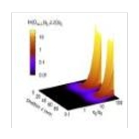 constants and the local quasi-Fermi level splitting using the detailed balance relation between local absorption and emission rates. The framework obtained in this way is shown to reproduce the generalized Kirchhoff relations between the luminescent emission from metal halide perovskite slabs under uniform excitation and the slab absorptance of light with arbitrary angle of incidence. Use of the proper local density of transverse photon states in the local emission rate includes cavity effects in the generalized Planck law for internal spontaneous emission, which are neglected in the conventional Van Roosbroeck-Shockley formalism and avoids spurious divergencies due to non-radiative energy transfer via longitudinal modes. Finally, a consistent treatment of re-absorption provides the local rate of secondary photogeneration required for the consideration of photon recycling in an opto-electronic device simulator that includes the effects of charge transport.
==============================
Assessment of Photon Recycling in Perovskite Solar Cells by Fully Coupled Optoelectronic Simulation
Simon Zeder, Beat Ruhstaller, and Urs Aeberhard
PHYSICAL REVIEW APPLIED
https://doi.org/10.1103/PhysRevApplied.17.014023
Abstract
An optical dyadic Green’s function framework to describe the transverse electromagnetic fields in a planar perovskite solar-cell stack is coupled to an electronic drift-diffusion model for rigorous treatment of 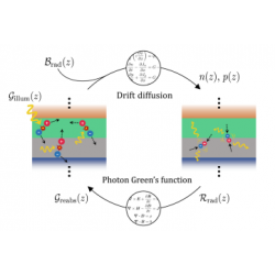 photon recycling in the wave-optics regime for a realistic photovoltaic device. The optical model provides the local reabsorption rate as well as a detailed-balance compatible radiative prefactor, which are used in the electronic model to achieve a self-consistent solution that yields the full optoelectronic device characteristics. The presented approach provides detailed insights into the impact of photon recycling on device performance under different regimes of charge transport and recombination and can help identify the various electronic and optical losses for nonideal, realistic devices. The global efficiency of photon recycling is quantified by defining quantum efficiencies of reabsorbed radiation, while the local efficiency can furthermore be quantified by defining an effective local radiative prefactor. The model introduced here can be used to guide the design of future devices that exploit the full potential of photon recycling.
==============================
The electronic stability of tin-halide perovskitecharged regions
Cameron Underwood,a Zhou Wang,b Guosheng Shao,b J. David Carey a and S. Ravi P. Silva
SCIENTIFIC REPORTS
https://10.1039/d1ma01232k
Abstract
We 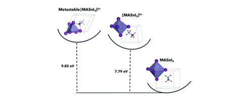 report on the evolution of the electronic structure and partial oxidation state of tin and iodine in ASnI3, where A = CH3NH3 (MA), CH(NH2)2 (FA) and Cs, with an aim to develop stable, long-term, non-toxic halide-perovskite solar cells. Although charge cannot be directly removed from specific elements, we show a reduction in the charge of primarily SnI3 in a hypothetical [ASnI3]2+ unit cell, which was calculated due to the valence band edge being dominated by Sn 5s and I 5p anti-bonding states, accompanied by a reduction in the unit cell volume of [ASnI3]2+ compared to ASnI3. The band structure calculations show semiconducting behaviour in ASnI3 with metallic behaviour in [ASnI3]2+, and similar behaviour is also found for APbI3 and [APbI3]2+, where the Pb atoms exhibit partial charge compared to Sn. This study allows for the analysis of localised charged regions, directing the contribution of the electronic states to stability in perovskite solar absorbers, such as interface recombination and deep trap states.
==============================
Ehsan Rezaee, Dimitar Kutsarov, Bowei Li, Jinxin Bi & S. Ravi P. Silva
SCIENTIFIC REPORTS
https://doi.org/10.1038/s41598-022-10790-z
Abstract
Halide perovskite materials have been extensively explored for their unique electrical, optical, magnetic, and catalytic properties. Most notably, solar cells based on perovskite thin films have improved their power conversion efficiency from 3.8% to over 25% during the last 12 years. However, it is still a challenge to develop a perovskite‑based ink, suitable for upscaling the fabrication process of high‑quality perovskite films with extreme purity, good crystallinity, and complete coverage over the deposition area. 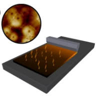 This is particularly required if the perovskite films are to be used for the scaled production of optoelectronic devices. Therefore, to make halide perovskites commercially available for various applications, it is vital to develop a reliable and highly robust deposition method, which can then be transferred to industry. Herein, the development of perovskite precursor inks suitable for use at low‑temperature and vacuum‑free solution‑based deposition processes is reported. These inks can be further tailored according to the requirements of the deposition method, i.e., we propose their use with the industrially viable deposition technique called “slot‑die coating”. Furthermore, a route for the preparation of low‑cost and high‑volume manufacturing of perovskite films on both rigid and flexible substrates is suggested in this paper. The presented approach is suitable for the fabrication of any functional layers of perovskites, that can be employed in various scaled applications, and it seeks the potential and the methodology for perovskite film deposition that is scalable to industrial standards.
==============================
Saeideh Farzaneh Kalourazi, Fei Wang, Haodong Zhang, Michael Selzer, and Britta Nestler
Journal of Physics: Condensed Matter
https://doi.org/10.1088/1361-648X/ac8b4d
Abstract
The porous microstructure has been widely observed in a variety of polymer solutions that have been broadly applied in many industry fields. Phase separation is one of the common mechanisms for the formation of the porous microstructure in binary polymeric mixtures. Previous studies for the formation of porous microstructures mostly focus on the separation of the bulk phase. However, there is a paucity of investigation for the phase separation of polymer mixtures contacting the solid substrate. 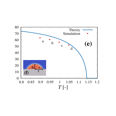 When the polymeric liquid mixtures interact with the solid substrate, the wetting boundary condition has to be taken into account. In this work, we present a phase-field model which is coupled with the wetting boundary condition to study the phase separation in binary polymer solutions. Our consideration is based on the polymerization-induced phase separation, and thermally induced phase separation by using the Flory–Huggins model. By taking the wetting effect into account, we find that polymer droplets spontaneously occur in the microstructure, even though the bulk composition is outside the spinodal region. This phenomenon is caused by the surface composition resulting from the wetting effect that was often overlooked in literature. For the phase separation in the binary polymer mixture, we also study the impact of the temperature gradient on the microstructural evolution. The porosity, the number of droplets, and the mean radius of the droplets are rationalized with the temperature gradient.
==============================
Camilla Vael, Sandra Jenatsch, Simon Züfle, Frank Nüesch and Beat Ruhstaller
Journal of Physics: Condensed Matter
https://doi.org/10.1063/5.0088426
Abstract
Thermally stimulated current (TSC) is a widely used technique to assess trap states and extract their density, energy, and capture rate using analytical expressions. In many cases, the latter are derived from physical models pertaining to inorganic semiconductors stipulating the absence of space charge or constant lifetime of free charge carriers. Especially for organic semiconductors, the validity of these equations can, therefore, be argued. Here, we investigate the validity range of this approach by fitting the classical equations to synthetic TSC data obtained from drift-diffusion simulation using representative input parameters for organic semiconductors  We find that the equation derived for slow recapture rate as well as the initial rise method provide excellent trap parameter predictions. On the other hand, the equation using the temperature of the peak current as well as the one derived for fast retrapping have a limited range of validity. An important merit of drift-diffusion modeling is the possibility to access local variables such as charge carrier density, electric field, and recombinaton. We unravel that a small fraction of traps nearby the electrode cannot be emptied even at high temperature due to the diffusion of charge carriers from the electrode into the semiconductor. Additionally, we find that an important electrostatic factor relates the extracted charge carriers measured by the external circuit and the input trap density. For the homogeneously distributed trap states used here, this factor is precisely two. Finally, extensions of the model are analyzed by implementing temperature and field dependent mobility into the drift-diffusion model.

![]()
This project has received funding from the European Union’s Horizon 2020 Research and Innovation Programme under Grant Agreement No 953187

